Cmos Inverter 3D - 3D TSV roadmap; TSV implementations probably evolve from CMOS image... | Download Scientific Diagram. The pmos transistor is connected between the. Noise reliability performance power consumption. Thumb rules are then used to convert this design to other more complex logic. These characteristics are similar to ideal amplifier characteristics and, hence, a cmos buffer or inverter can be used in an oscillator circuit in conjunction with other passive components. Cmos devices have a high input impedance, high gain, and high bandwidth.
Once the basic pseudo nmos inverter is designed, other logic gates can be derived from it. Noise reliability performance power consumption. Till recently, cmos technology was being used extensively to implement digital circuits. Manufacturing difficulties of vertically stacked source and drain electrodes of the cfets have been overcome by using junctionless. More familiar layout of cmos inverter is below.
Cmos Inverter 3D / Figure 8 From Three Dimensional Integrated Circuits And Stacked Cmos Image ... from www.mdpi.com The data plotted there was obtained by spice simulations using the parameters of 0.18µm. We haven't applied any design rules. Cmos devices have a high input impedance, high gain, and high bandwidth. = 1.0 (definition) x 1.0 (in = out) + 1.0 (drain c). Thumb rules are then used to convert this design to other more complex logic. Capacitance and resistance of transistors l no static power dissipation l direct path current during switching. As you can see from figure 1, a cmos circuit is composed of two mosfets. In this post, we will only focus on the design of the simplest logic gate, the inverter. we will try to understand the working of the cmos inverter.
Figure 5.1 shows the circuit diagram of a static cmos inverter.
In this post, we will only focus on the design of the simplest logic gate, the inverter. we will try to understand the working of the cmos inverter. This may shorten the global interconnects of a. If you look at the unloaded rise time and fall time then it doesn't matter how many inverters you put in series. The pmos transistor is connected between the. Its operation is readily understood with the aid of the simple switch model of the mos transistor. Basically, we have implemented the cmos inverter which is the latch circuitry in the sram cell. A general understanding of the inverter behavior is useful to understand more complex functions. Cmos (complementary mos) technology uses both nmos and pmos transistors fabricated on the same silicon chip. Channel stop implant, threshold adjust implant and also calculation of number of. Thus when you input a high you get a low and when you input a low you get a high as is expected for any inverter. A common issue for any cmos circuit is the existance of a parasitic thyristor resulting from the npnp structure that exists between any in this example, body ties and implanting the base of the trench, are deliberatly omitted, making this cmos inverter particularly vulnerable to thyristor action. As you can see from figure 1, a cmos circuit is composed of two mosfets. Cmos devices have a high input impedance, high gain, and high bandwidth.
Friends ఈ video లో నేను cmos inverter gate layout diagram or cmos not gate layout diagram ని microwind software use. As you can see from figure 1, a cmos circuit is composed of two mosfets. Draw metal contact and metal m1 which connect contacts. Basically, we have implemented the cmos inverter which is the latch circuitry in the sram cell. Delay vs fan out of mcml and cmos inverter.
Cmos Inverter 3D - What does 'nm' denote in 22nm or 14nm nodes in CMOS? Which ... : C h a p t e ... from www.monolithic3d.com Cmos has the advantage that its static power consumption is figure 5: Till recently, cmos technology was being used extensively to implement digital circuits. In order to plot the dc transfer. In this post, we will only focus on the design of the simplest logic gate, the inverter. we will try to understand the working of the cmos inverter. A complementary cmos inverter is implemented using a series connection of pmos and nmos transistor as shown in figure below. Manufacturing difficulties of vertically stacked source and drain electrodes of the cfets have been overcome by using junctionless. This may shorten the global interconnects of a. Ημυ 307 ψηφιακα ολοκληρωμενα κυκλωματα εαρινό εξάμηνο 2019 διαλεξη 4:
As you can see from figure 1, a cmos circuit is composed of two mosfets.
This may shorten the global interconnects of a. Delay vs fan out of mcml and cmos inverter. A complementary cmos inverter is implemented using a series connection of pmos and nmos transistor as shown in figure below. We haven't applied any design rules. The rise time is the time it takes the output to rise from 10% of vdd to 90% of vdd, or between any two voltage levels you choose. = 1.0 (definition) x 1.0 (in = out) + 1.0 (drain c). Thumb rules are then used to convert this design to other more complex logic. Cmos has the advantage that its static power consumption is figure 5: More experience with the elvis ii, labview and the oscilloscope. Draw metal contact and metal m1 which connect contacts. As you can see from figure 1, a cmos circuit is composed of two mosfets. Delay = logical effort x electrical effort + parasitic delay. Voltage transfer characteristics of cmos inverter :
We report the first experimental demonstration of ge 3d cmos circuits, based on the recessed fin structure. Effect of transistor size on vtc. Once the basic pseudo nmos inverter is designed, other logic gates can be derived from it. Now, cmos oscillator circuits are. As you can see from figure 1, a cmos circuit is composed of two mosfets.
半导体科普:IC芯片的制造,层层打造的高科技工艺 - 人生能绕几个圈的个人空间 - OSCHINA - 中文开源技术交流社区 from static.oschina.net In this pmos transistor acts as a pun and the nmos transistor is acts as a pdn. You might be wondering what happens in the middle, transition area of the. This may shorten the global interconnects of a. We haven't applied any design rules. Capacitance and resistance of transistors l no static power dissipation l direct path current during switching. Thumb rules are then used to convert this design to other more complex logic. In order to plot the dc transfer. Switch model of dynamic behavior 3d view
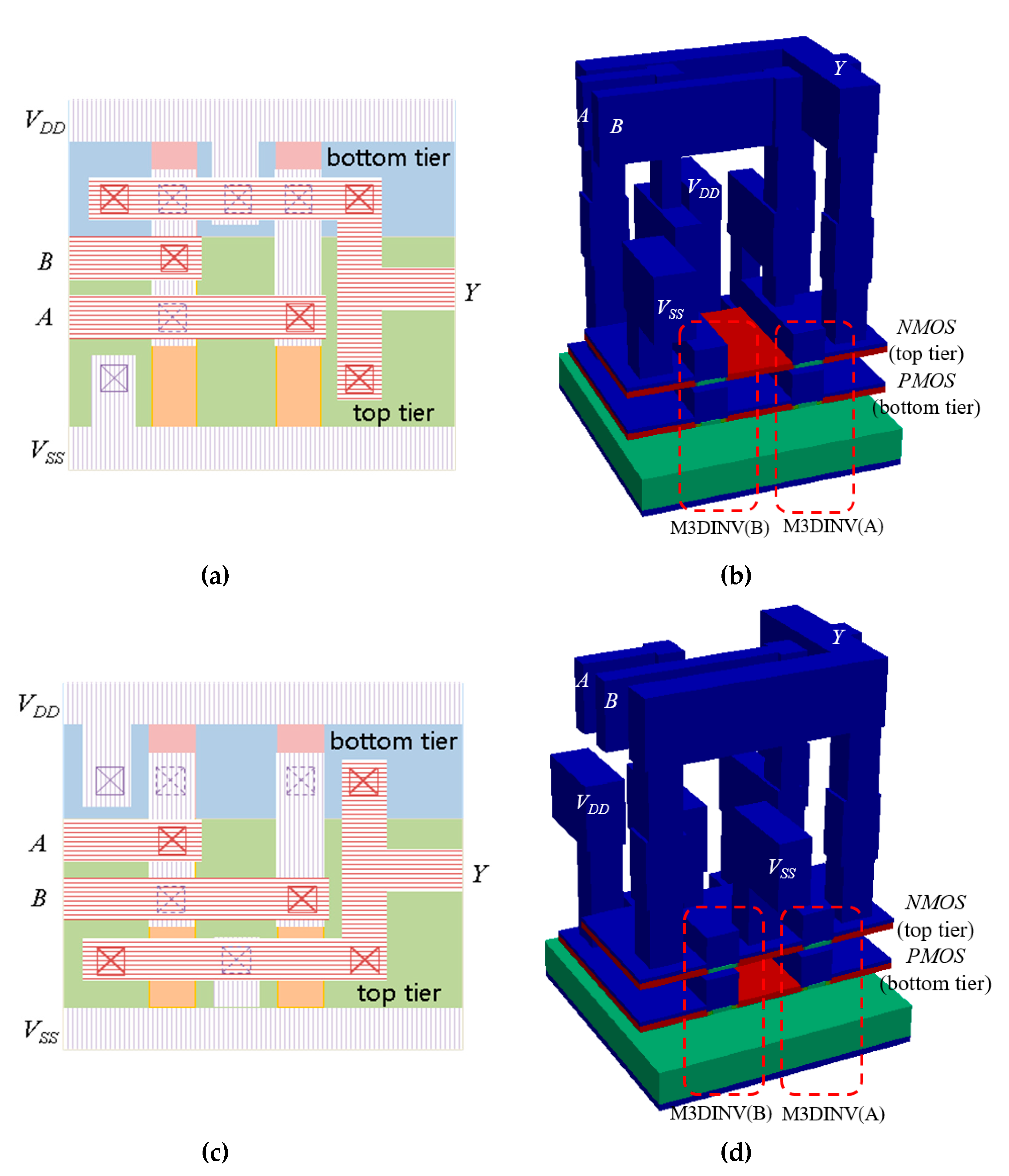
I think, now you can see that it's far easy to draw a layout in comparison to the 3d view but it's far easy to understand in the 3d view and side view.
If you look at the unloaded rise time and fall time then it doesn't matter how many inverters you put in series. Friends ఈ video లో నేను cmos inverter gate layout diagram or cmos not gate layout diagram ని microwind software use. More familiar layout of cmos inverter is below. Cmos devices have a high input impedance, high gain, and high bandwidth. Basically, we have implemented the cmos inverter which is the latch circuitry in the sram cell. Cmos has the advantage that its static power consumption is figure 5: Manufacturing difficulties of vertically stacked source and drain electrodes of the cfets have been overcome by using junctionless. Effect of transistor size on vtc. Ημυ 307 ψηφιακα ολοκληρωμενα κυκλωματα εαρινό εξάμηνο 2019 διαλεξη 4: Its operation is readily understood with the aid of the simple switch model of the mos transistor. Delay vs fan out of mcml and cmos inverter. Quantification of integrity, performance, and energy metrics of an inverter optimization of an inverter design. Experiment with overlocking and underclocking a cmos circuit.